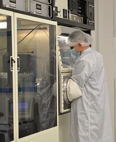
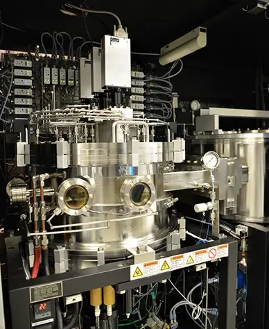
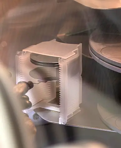
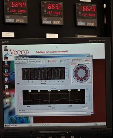
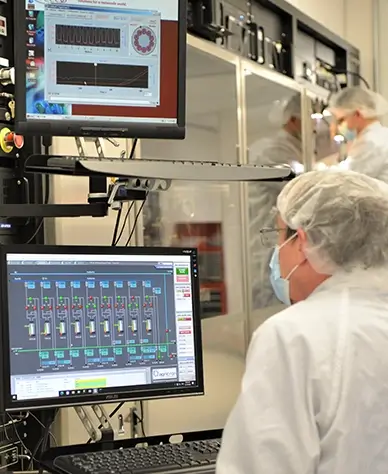
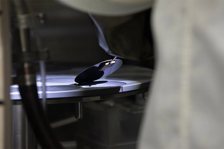
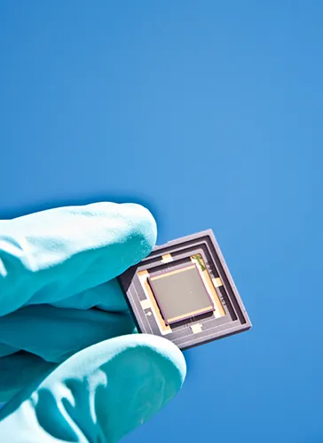
At Masimo Semiconductor, our extensive MOCVD experience and capacity enable us to grow a wide range of GaAs and InP epitaxial structures to our customers’ designs. We recognize that time-to-market is critical to our customers’ success, so we strive to provide the fastest turnaround times possible. Our epitaxy scientists and engineers work closely with customers to develop and improve proprietary structures for specific applications.
MOCVD Materials
InP
InGaAs
InAlAs
InAs
InAsP
InGaAlAs
InGaAsP
GaAs
AlGaAs
InGaAlAs
GaAsP
AlGaP
AIGaAsP
InGaP
InAIP
InAIGaP
Typical Devices
Plasma filters
Laser power converters
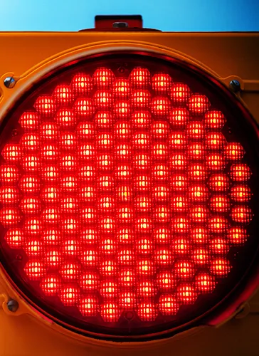
LEDs/RCLEDs (visible to IR)
DH, QW, DFB lasers (visible to IR)
VCSELs (visible to IR)
Detectors
Thermophotovoltaics
QWIPs
HBTs – modulators
Photocathodes
PIN
SJ, MJ Solar cells, CPVs
HEMTs, FETs
High Power lasers
High Speed lasers
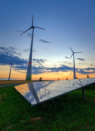
Typical Applications
Sensors
3D sensing
Infra-red cameras
Wireless communications
Wireless power conversion
Thermal power conversion
GPS
LiDAR
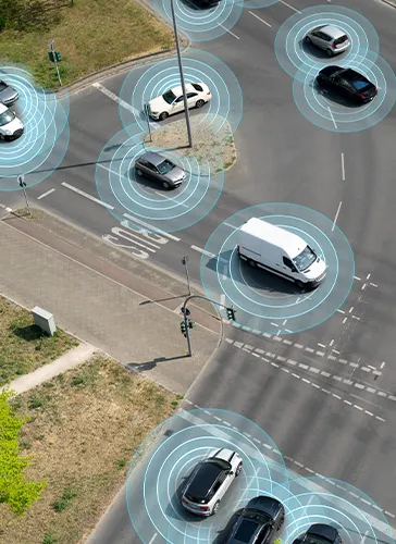
Automotive
Medical systems
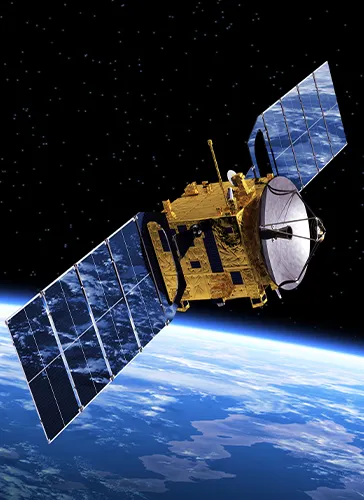
Satellite systems
Solid state lasers
Fiber amplifiers
Displays
High Power lasers
High Speed lasers
Illumination
Pointers
Mouses
Cameras
Cell phones
Custom Applications Are Our Specialty
We can provide the following characterization data for our epitaxial wafers (or witness wafers, as appropriate).
Nomarksi surface inspection, Surfscan defect count and haze