Technology

Device Testing

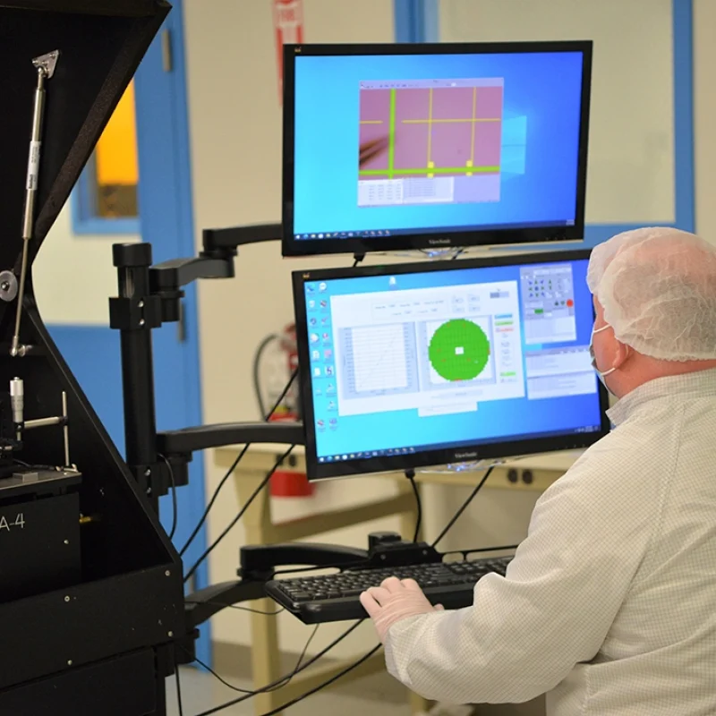
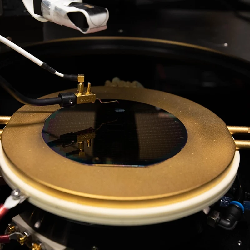
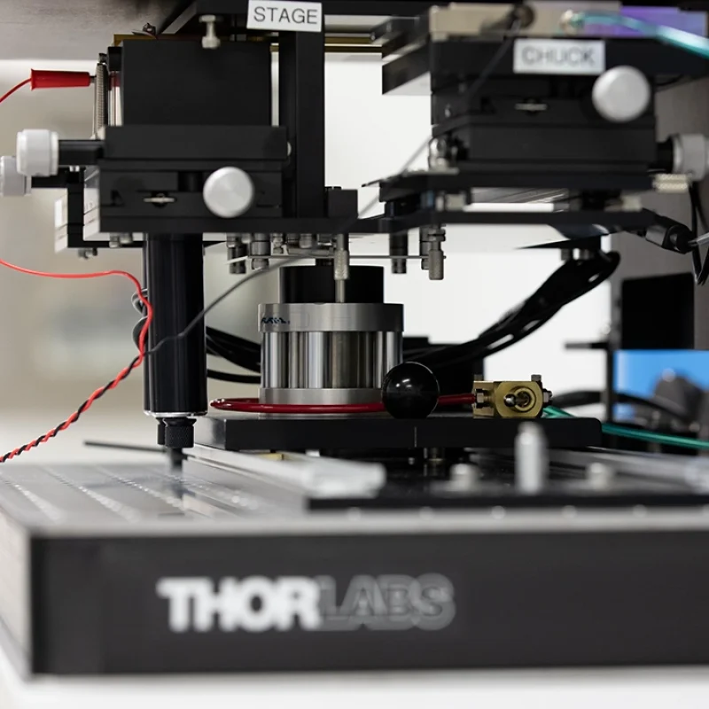
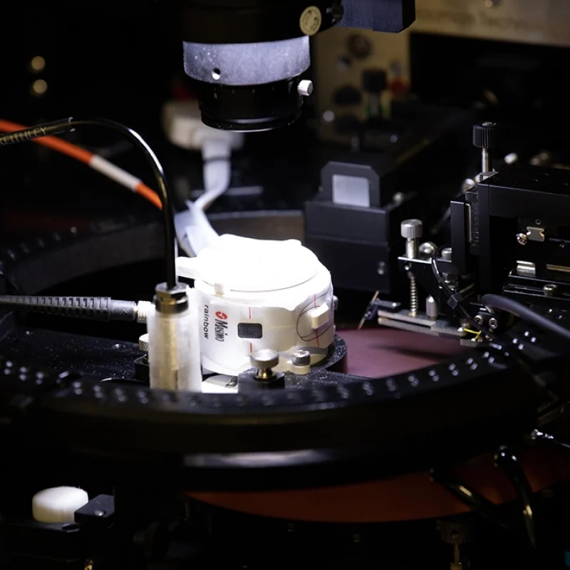
Materials Characterization and Final Test Facility

An essential element in developing improved products and maintaining the quality of our production is our extensive material characterization and final test facility. Masimo Semiconductor has extensive in-house instrumentation and test equipment.

In-House Instrumentation

Double crystal x-‍ray diffraction

• Layer thickness
• Composition

Polaron and Hall carrier concentration

Automated on-‍wafer device test
cycle icon

Photoluminescence & reflectivity mapping

• Spectral response
• Quantum efficiency
• VCSEL maps

Normarski microscopy

Surfscan defect and haze data

Device Test

  • Quantum Efficiency Measurements
  • Automated Wafer Testers (PIV and Spectrum of LEDs, VCSELs, PD dark current)
  • Solar Simulator (illuminated IV tests of photovoltaics and LPCs)
  • Flash Solar Simulator (concentration to 1000 suns for solar cells)

View a list of available brochures and request additional information.